| Vacuum Tube Preamplifier
Analysis and SPICE Simulation
Michael S. McCorquodale
ABSTRACT
This paper investigates the analysis and simulation of a common cathode preamplifier stage. The concept of an AC model for the triode is presented and the equivalent circuit technique is described. Theoretical calculations for amplifier gain and frequency response are derived and compared to simulation results in the SPICE3 environment where good agreement is shown. DATA SHEET
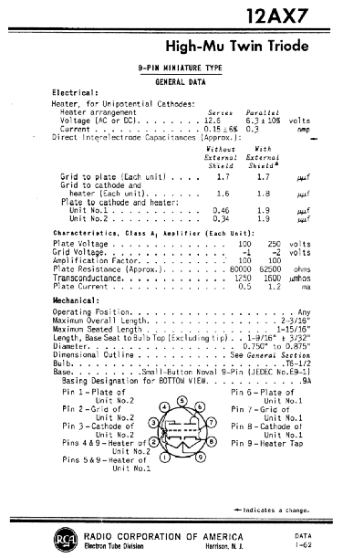
Sections of the following data sheet will be referenced throughout the analysis that follows. This data sheet was scanned from the original RCA data sheets that were available during the production of RCA vacuum tubes.
Data Sheet 1: RCA 12AX7 DATA SHEET [DOWNLOAD]
ANALYSIS
Prior to performing analysis it is imperative to observe that there are two types of signals present in any analog amplifier circuit and the properties of each are not identical. The composite signal present in an amplifier circuit is comprised of AC and DC components. The DC components are commonly denoted by capital letters. For example, the DC plate current is represented by IP. The AC components are denoted by lower case letters and correspondingly the AC plate current is represented by ip. Voltages follow an identical form of notation. Fig.1 illustrates these AC and DC components, using the notation described, for a common cathode amplifier stage. 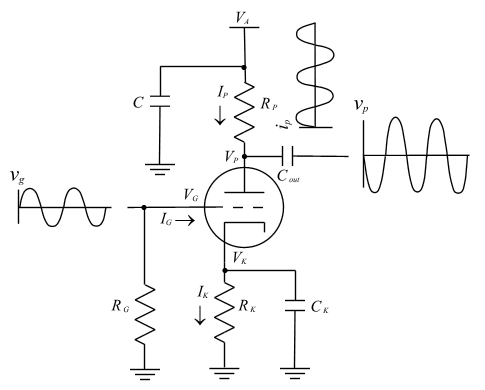
Fig 1: AC AND DC COMPONENTS IN A COMMON CATHODE AMPLIFIER STAGE The characteristic properties of AC and DC signals are apparent from fundamental circuit theory. As an example, a capacitor behaves as a DC block. However, it will pass AC signals in general, but the transfer will be contigent upon signal frequency, type of capacitor, and total capacitance. Here it should be noted that these differences are attributed to the mechanism of current flow in each case. DC signals move charge by conduction. Electrons from one part of the circuit travel continuously to another point due to an electric field that is created by a potential difference, or voltage. Once the capacitor is charged up by the conduction of charge to each plate, the capacitor appears as an open circuit to DC signals. By contrast, AC signals move through capacitors by the mechanism of displacement. Small amounts of charge are moved to and from the plates of the capacitor. They are not conducted through the capacitor. However, this displacement of charge is the means by which AC signals propagate through capacitors. Lastly, it is important to understand that the AC signal is superimposed upon the DC signal and thus the two components obey the mathematical laws of superposition: namely, the AC and DC components can be considered separately and superimposed. However, it should be noted that this is only true to a first order since AC nonlinearities in the tube will give rise to DC components, but this is beyond the scope of this paper. It is equally important to recognize that the two components are interrelated. This will become apparent shortly. Begin by recalling the common cathode configuration, shown in Fig. 2, which is commonly implemented in tube preamp circuitry. 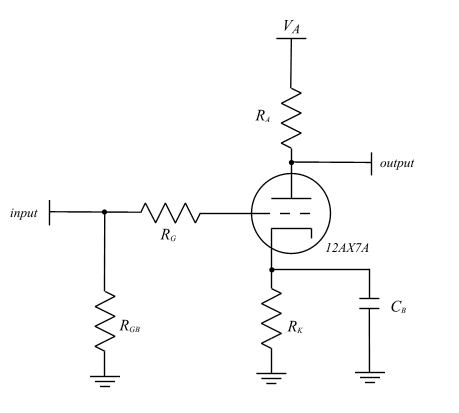
Fig. 2 THE COMMON CATHODE CONFIGURATION It is important to understand the purpose of each element in the configuration. The grid bias resistor, RGB, provides a high resistance (DC) path to ground and thus it biases the grid to zero volts DC. Moreover, it sets the input resistance into the amplifier. It is generally desirable for the input resistance of an amplifier to be as high as possible so the input signal is not attenuated by the voltage divider set up by the amplifier input resistance and signal source resistance. The bypass capacitor, CB, provides an AC path from the cathode to ground. Therefore, the cathode resistor, RK, does not influence the AC signal since the cathode is effectively an AC ground. The grid resistor, RG, limits the frequency response of the amplifier by interacting with the capacitance between the grid and plate to create an RC circuit with a -3dB point, or half power point, of about 20kHz as will be shown later. This will damp any oscillations that may occur at higher frequencies and therefore stablize the amplifier. The plate and cathode resistors simply limit the DC current in the tube, or more specifically, they are what set the bias point. However, these components will also set the gain as will be shown. Next, it is instructive to define certain AC parameters of the tube so an AC model, more commonly called a small signal model, may be derived. Be aware that the small signal model is exactly that: a model. Models are intended to approximate the real physical operation of a device. The operation of tubes, or any device for that matter, is rather complex and nonlinear in general. However, if one can represent the operation of the device by familiar and simple linear circuit elements, such as resistors and capacitors, then the model may make analysis much easier. These parameters that are defined below are inherent to the model and bear no real significance except for providing a method for notating the physical properties of the device. The parameters are as follows.
Equations 1: SMALL SIGNAL MODEL PARAMETERS Here rp is the dynamic plate resistance, gm is the mutual conductance, and m is the amplifier gain. Do not confuse m with the actual gain of the circuit. This parameter actually quantifies the open loop, or unloaded, gain of the amplifier. Thus m is actually the maximum achieveable gain. For those unfamiliar with calculus, the ¶ operator represents a partial derivative of a multivariable function with respect to the variable in the denominator. This can be thought of as a differential change or a very small change of one parameter with respect to the other. The straight bar means while holding constant. So in words, the dynamic plate resistance, rp, is a small change in the plate voltage with respect to a small change in the plate current while holding the control grid voltage constant. Mutual conductance is often misunderstood, but if the definition is simply explained in words as above, it becomes less confusing. The mutual conductance is the change in plate current with respect to grid voltage while holding the plate voltage constant. What does this mean? Well, it is simple. If the grid voltage changes just a little bit, then a small amount of change in the plate current is induced. The ratio of this is the mutual conductance. This is fundamental to tube operation. The control grid controls the current from the plate to cathode. Here we have simply quantified that fact. The role of gm will be apparent in the small signal model. We are now ready to discuss the aforementioned small signal model. The small signal model makes use of these differential parameters. Although there is no absolute definition of what a small signal is, it is safe to assume that the audio signal is always small in preamp circuitry. A more rigorous definition that holds generally is that a small signal must incur no more than 5% THD, or total harmonic distortion. Please note that power amp stages cannot be modeled by this small signal model since the signal is large and the differential parameters do not apply. There are some simple rules for determining the small signal equivalent circuit. This is to be done only for analysis by hand and therefore do not actually do this to a circuit. The rules are as follows:
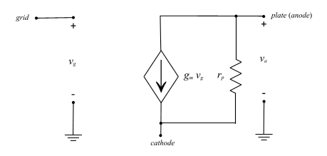
Now to examine the small signal models for the triode. Note that the triangular source represents a dependent source. Its value depends on other circuit parameters, namely the grid voltage. It should also be noted that these are midband models. There are no capacitive model parameters shown here and thus there are no frequency dependent devices in the model. Although this is a very simple model, it is accurate for determining the midband gain, or the gain at middle frequencies, by hand. However, these parasitic capacitances are included in the models that are used later to determine the frequency response of this circuit. The appropriate values of these parasitics are obtainable from manufacturer's data. However, we will not address these additions to the model here since they will only confound hand calculations of the gain. In Fig. 3A the small signal model makes use of a dependent voltage source. Thus, when a grid voltage is applied, a corresponding plate voltage is induced that is multiplied by m. The plate resistance is then in series with this source. The Norton equivalent of this circuit can be derived by simply replacing the voltage source with an equivalent current source in parallel with the plate resistance. It should be clear that the two models are identical. For example, using the dependent voltage source model will yield a plate voltage of -mvG. By comparison, a plate voltage of -gmvGrp can be determined using the dependent current source model. Of course the product gmrp is simply m and thus the two models are equivalent. 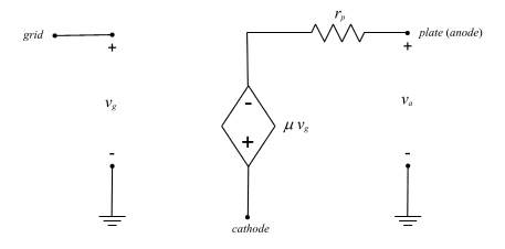
(A)
Fig. 3 THE TRIODE SMALL SIGNAL MODEL (A) USING A DEPENDENT VOLTAGE SOURCE (B) USING A DEPENDENT CURRENT SOURCE As described previously, parasitic capacitors exist between each terminal of the tube. These capacitors are illustrated in Fig. 4. 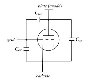
Fig. 4: TRIODE PARASITIC TERMINAL CAPACITORS It is trivial to include these elements in the small signal model. The modifications for the dependent current source model are shown in Fig. 5. 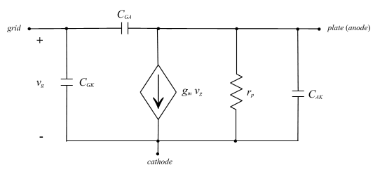
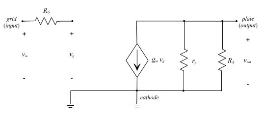
Fig 5: THE DEPENDENT CURRENT SOURCE SMALL SIGNAL MODEL INCLUDING PARASITIC CAPACITANCORS One may wonder why in this model the capacitors are not short circuits to the AC signal. This is due to the fact that these capacitors do effect the AC signal. They are inherent to the triode and by including them, the model becomes more accurate the frequency response of the device can be determined. The capacitors that were shorted previously were bypass capacitors and thus are typically very large so the AC impedence is very small and thus these capacitors behave as short circuits. The parasitic capacitors in the model above are are small by comparison and thus the associated impendence is not negligible. Now let's look at our model for the common cathode using the rules for determining the small signal model. Fig. 6A shows the midband model, which will be used to determine the gain, while Fig. 6B shows the model with the parasitic capacitors which will be used to find the cut-off, or -3dB, freqeuncy. In both figures, the dependent current source model has been selected since it is easiest to analyze. However, the dependent voltage source model could also be employed. 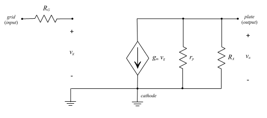
(A) 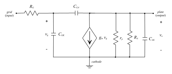
(B) Fig. 6: COMMON CATHODE CONFIGURATION UTILIZING CURRENT SOURCE EQUIVALENT MODEL (A) MIDBAND MODEL (B) MODEL INCLUDING PARASITIC CAPACITORS To find the gain we simply need to find the output current and then combine resistances in parallel. We readily notice from the model how a negative sign will be introduced into the gain equation. This is a function of the control grid's operation as described previously. Now to perform the analysis. The voltage at the plate, or output, will be the product of the current to the output and the parallel combination of rp and RA. Of course the current to the output is simply gmvg and thus the gain is simply vout/vg. The derivation of the final gain expression is shown below where Av denotes the voltage gain.
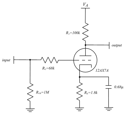
Equation 2: GAIN CALCULATION In the expressions above the operator || represents the parallel combination of resistances. It is important to note that the amplification factor (m), the mutual conductance (gm), and the dynamic plate resistance (rp) are functions of the bias point as can can be seen in the data sheet at the beginning of this paper. This is exactly where the interdependence between the DC and AC signals lies. It should be apparent that RA is incorporated into the final gain equation. Clearly changing RA will change the bias point, which will also change the AC model parameters and hence the gain. Prior to performing a SPICE simulation, an example is presented. Examine the circuit below.
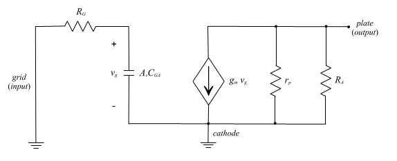
The current source AC midband model is shown in Fig. 8A for this circuit. In Fig. 8B an equivalent AC model is presented. It is well known that in the common cathode configuration, the input-to-output capacitance dominates the frequency response. Of course, the corresponding capacitor from input-to-output is CGA. Using the well known Miller's Theorem, this feed-forward capacitor can be modeled by an equivalent input capacitor that is multiplied by the gain of the stage and is in shunt with the input signal. The technique known as Open Circuit Time Constants (OCTC) was used to arrive and the model shown in Fig. 8B. These concepts can be further investigated in any elementary circuits text.
Fig. 8: (A) SMALL SIGNAL EQUIVALENT CIRCUIT (B) SMALL SIGNAL EQUIVALENT USING MILLER'S THEOREM >For these parameters, the bias current will be about 1.2mA and thus by looking at the data sheet at the top of this paper, the plate resistance and mutual conductance can be determined. They are 62.5k and 1.6mmhos respectively. The gain is then calculated as follows:
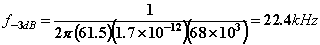
Equations 3: NUMERICAL GAIN CALCULATIONS Clearly the analysis is trivial once it is understood. The -3dB frequency is calculated by noting that the RC time constant associated with the input grid resistance and Miller capacitor dominates the frequency response. Thus the RC time constant associated with these devices can be calculated and the -3dB frequency is determined by taking the reciprocal of this time constant and converting from radians to Hertz. The value of CGA is obtained from the data sheet at the beginning of this paper.
Equations 4: -3dB FREQUENCY CALCULATION Again the analysis is trivial once it is understood. SIMULATION
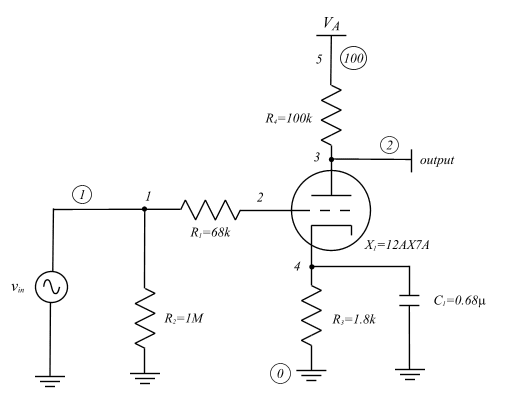
Although the previous analysis was trivial, using a more complex model would increase the difficulty of analysis. Doing so is not insughtful since the purpose of hand calculations is to simply determine that parameters that most significantly effect the amplifier performance and then make adjustments accordingly. Therefore, utilizing a simulation program is an indispensible tool since the designer can increase the complexity and accuracy of the model without increasing the design time due to the efficiency of computer processing. The SPICE3, or Berkeley SPICE, package was utilized for the simultions that follow. This paper will not address SPICE netlist format or the use of SPICE3, but there are numerous references that can aid the reader in understanding the usage of SPICE programs. SPICE3 can be purchased for around $100 from the University of California at Berkeley. Please note that the model used for the triode in the netlist that follows is SPICE3 compatible, but is most likely compatible with other simulators. Also see the links on the previous page for information on SPICE3 and the Windows95/98/00/NT port of SPICE3 or just download the port here: [DOWNLOAD] Below is a schematic of the circuit to be simulated. The circled numbers refer to the nodes in the netlist at the top of the hierarchy. The uncircled numbers refer to the nodes within the preamplifier model.
The corresponding netlist for this circuit follows. The
supply voltage, VA,
was selected to be 350V in order to set the current to about 1.2mA.
Table 1: PREAMPLIFIER CIRCUIT NETLIST [DOWNLOAD] Three different simulations were performed: OP, Transient,
and AC. The OP analysis provides the DC operating currents and voltages.
Transient analysis determines the response in the time domain and AC analysis
shows the frequency response, or the gain over frequency. Results of the
OP analysis are shown in Table 2.
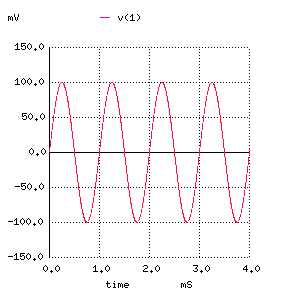
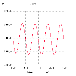
Table 2: DC SIMULATION RESULTS Here, i(va) is the current drawn from the supply. Thus, the bias current is about 1.1mA and this is very close to the desired point of 1.2mA. v(1) is the grid voltage and it is, of course, biased to ground via the 1M resistor. There is no grid current, as shown by i(vin) since vin is connected directly to the grid. The plate voltage, v(2), is at about 240V while the supply voltage, v(100), is at 350V. Though this bias point is not exactly the same as the point desctibed in the data sheet the bias is close enough to justify the use of the AC parameters used in the prvious analysis. The transient analysis provides the time domain response
for a given input. Note that the input signal, v(1), was slected to be
100mV and 1kHz. The output signal, v(2), shows significant amplification
at the plate. By rough estimates, the gain is around 50 since the output
is swinging just over 5V zero-to-peak for a 100mV zero-to-peak input.
Fig. 10: TRANSIENT SIMULAITON RESULTS (A) INPUT SIGNAL (B) OUTPUT SIGNAL This appriximate gain result is quite close to the results
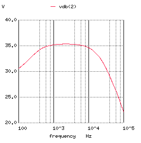
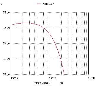
obtained by hand calculations. By performing an AC analysis, the frequency
response of the preamplifier is determined. The results are shown in Fig
11.
Fig. 11: AC SIMULATION RESULTS (A) FROM 10 TO 100kHz (B) ZOOMED PLOT SHOWING -3dB FREQUENCY The gain is very flat over the frequencies of interest for guitar audio amplification. Moreover, we can see that the gain is indeed about 35dB in the midband which is almost identical to the hand calculation. In Fig. 6B, the frequency response is zoomed and we can see that the frequency at which the gain rolls off 3dB is just over 20kHz. Again, these results correspond well with the theoretical calculations. CONCLUSION
This paper examined significant aspects of amplifier analysis and simulation. It is critical for the designer to be able to analyze each stage accurately, be it by hand or with a simulation program. The discussion presented here can be extended to many different amplifier configurations. Clearly the advantage of analysis and simulation prior to amplifier construction is the ease at which modifications can be made to obtain the desired results. REFERENCES
Louis N. Ridenour et al., Vacuum Tube Amplifiers, 1st ed., Massachusetts Institute of Technology Radiation Laboratory Series, New York: McGraw-Hill Book Company, 1948. Alfred J. Cote Jr. and J. Barry Oakes, Linear Vacuum-Tube and Transistor Circuits: A Unified Treatment of Linear Active Circuits, New York: McGraw-Hill Book Company, 1961. Karl T. Compton et al., Magnetic Circuits and Transformers, New York: John Wiley & Sons, 1950. K. O'Connor, The Ultimate Tone, Canada: London Power Press, 1995. F. Langford-Smith et al., The Radiotron Designer's Handbook, 4th ed., Sydney: Wireless Press, 1953. Paul R. Gray and Robert G. Meyer, Analysis and Design of Analog Integrated Circuits, New York: John Wiley & Sons, 1993. Ron M. Kielkowski, SPICE: Practical Device Modeling, New York: McGraw-Hill Book Company, 1995. |