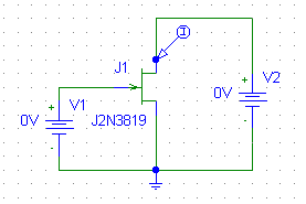
IV Plot circuit for a 2N3819 JFET
IV Plot circuit for a 2N3819 JFET
The tut_spice3_jfet_bias_iv.cir file for this spice circuit and dc analysis would be:
* Jfet DC nest sweep
V1  Ngate  0       DC 0
V2  Ndrain 0       DC 0

J1  Ndrain Ngate 0 J2N3819

.model J2N3819 NJF(Beta=1.304m Rd=1 Rs=1 Lambda=2.25m Vto=-3
+ Is=33.57f Cgd=1.6p Pb=1 Fc=.5 Cgs=2.414p Kf=9.882E-18 Af=1)

* Nest DC sweep
.DC V2 0 20 .1 V1 -2.6 0 0.2
.END
Shown below as Figure 1 is the characteristic I-V plot for the 2N3819 n-channel JFET.
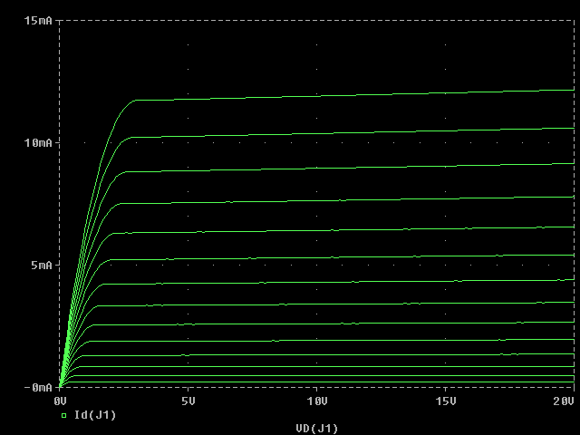
Figure 1 - The Spice IV Plot for a 2N3819 JFET
unix> spice3

Spice 1 -> source tut_spice3_bias_iv.cir

Spice 2 -> listing physical

        * Jfet DC nest sweep


     1 : * jfet dc nest sweep

     2 : v1  ngate  0       dc 0

     3 : v2  ndrain 0       dc 0

     4 : j1  ndrain ngate 0 j2n3819

     5 : *

     6 : .model j2n3819 njf(beta=1.304m rd=1 rs=1 lambda=2.25m vto=-3

     7 : + is=33.57f cgd=1.6p pb=1 fc=.5 cgs=2.414p kf=9.882e-18 af=1)

     8 : *

     9 : * nest dc sweep

    10 : .dc v2 0 20 .1 v1 -2.6 0 0.2

    12 : .end


Spice 3 -> run

Spice 4 -> display

Title: * Jfet DC nest sweep

Name: dc1 (DC transfer characteristic)


    j1#drain            : voltage, real, 2800 long
    j1#source           : voltage, real, 2800 long
    ndrain              : voltage, real, 2800 long
    ngate               : voltage, real, 2800 long
    sweep               : voltage, real, 2800 long [default scale]
    v1#branch           : current, real, 2800 long
    v2#branch           : current, real, 2800 long
Note that the first line starts the spice program within Unix. Line 1 reads in the spice source net list.
These two lines can be combined into a single command: spice3 source tut_spice3_bias_iv.cir.
Line 2 just displays the read in source file and which can be useful at times. Line 3 runs all the
analysis control statments within the read in file (.dc, .ac, .trans, ...). Line 4 displays the internal
variables for plotting.
Spice 5 -> set hcopydevtype=postscript

Spice 6 -> plot -v2#branch
Line 5 sets the plotting format for postscript printers. Line 6 plots the dc analysis using the negative of the V2 current.
A plot should now appear on the screen and press the button "hardcopy". The following message will appear:The file "/tmp/hcXXXX" may be printed on a postscript printer. Where XXXX is a number generated by the plot program. Now, in order to print to a postscript printer within spice use the shell command as follows
Spice 7 -> shell lpr /tmp/hcXXXX

Spice 8 -> quit
First of all, we want the amplifier to work in a linear region to minimize the amount of signal distortion. The optimal region for the JFET is in the constant current region. We also want to maximize the output range of our amplifier. If the Q point is too close to the pinchoff voltage, or the supply voltage, the signal will clip much sooner then if it were farther away from those two voltages. For these two reasons, the device is typically set up to operate at midpoint bias. This means that the JFET is biased so that the drain-source voltage is halfway between the supply voltage and the pinchoff voltage.
Another concern of the circuit is power consumption. Since the DC bias of the circuit consumes a certain amount of power which is not "useful" to the circuit (output as signal power), the power consumption should be minimized. This can be done by using as small a drain current as necessary to do the job that the amplifier needs to do.
The above points will be useful to you later on, since you've lucked out and had the Q point specified for you in both the homework and laboratory experiment. For this tutorial, I will use a Q point with a drain current of approximately 5 mA and a drain-source voltage of approximately 11 V.
Once the Q point has been chosen, the only other parameter of the circuit is the supply voltage, which was probably already known, and a factor in the selection of the Q point. For this tutorial, I will use a supply voltage of 20 V.
The next step is to draw a line from the X intercept at the supply voltage point, through the Q point, all the way to the Y axis. This is the DC load line, which the circuit will always operate along.
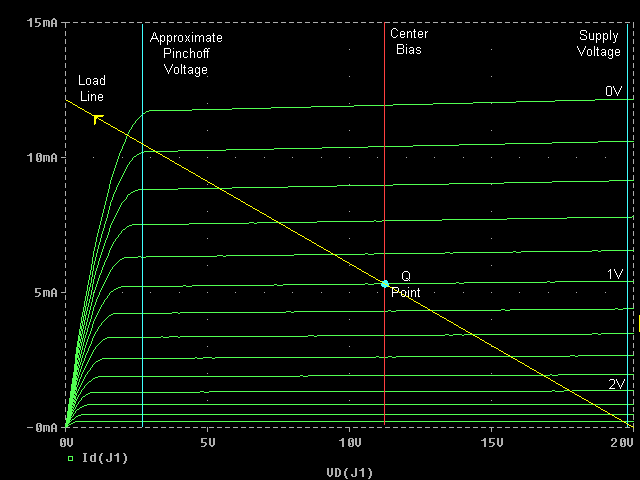
Figure 2 - DC Load Line for Amplifier
The preliminary work is now complete, and we are ready to begin selecting the components necessary to complete the circuit. The first step is to select the total amount of resistance necessary for the circuit to follow this line. This is calculated by dividing the x intercept (voltage) by the y intercept (current). 20 V / 12.12 mA = 1650 ohms
To bias the gate at the proper voltage (-1V according to the I-V plot), we need to add a source resistor according to the formula Vgs = -IdRs. For this circuit Rs = -1V/-(5.333 mA) = 188 ohms
This means that the remaining 1275 ohms of the 1650 will be added to the circuit as the drain resistance. The design of the circuit is now complete.
The operating point of the circuit can be verified by running a SPICE simulation. As you can see from Figure 3, the drain current is 5.319 mA, and the drain-source voltage is 11.22 V. These values are almost identical to the actual location of the Q point on the load line in Figure 2.
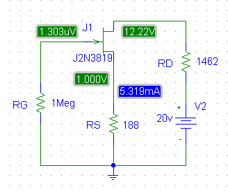
Figure 3 - SPICE Simulation of Circuit
Spice allows circuits to be grouped. This allows for good design techniques. Figure 3 is make into a subcircuit file, tut_spice3_jfet_bias.subckt, and is referenced by a .include and the X device statement inside the analysis file, tut_spice3_jfet_bias_dc.cir. The following shows how to get the bias values in Spice.
unix> spice3
 tut_spice3_jfet_bias_dc.cir

Spice 1 -> op

Spice 2 -> display


Here are the vectors currently active:

Title: * Jfet Gain-bandwidth plot
Name: op1 (Operating Point)

    amp1:nsource        : voltage, real, 1 long
    j:amp1:1#drain      : voltage, real, 1 long
    j:amp1:1#source     : voltage, real, 1 long
    v1                  : voltage, real, 1 long
    v1#branch           : current, real, 1 long
    vdd                 : voltage, real, 1 long [default scale]
    vdd#branch          : current, real, 1 long
    vin                 : voltage, real, 1 long
    vout                : voltage, real, 1 long


Spice 3 -> print vdd#branch

vdd#branch = -5.33131e-03

Spice 4 -> print -i(vdd)

-i(vdd) = 5.331305e-03

Spice 5 -> print Vin

vin = 1.327274e-05

Spice 6 -> print j:amp1:1#drain

j:amp1:1#drain = 1.220031e+01

Spice 7 -> print j:amp1:1#source

j:amp1:1#source = 1.005310e+00
Note line 1 determines the dc operating point of the circuit. This can also be placed in the circuit file as .OP and a run command issued in Spice. Line 2, the display shows all the nodes that can be measured. Lines 3 and 4 display the same information by using two different format commands.
Spice only gives the current values for a limited number of devices. A spice trick is to insert a zero dc voltage source in between the desired wire and then measure the current of this zero voltage source.
|
Usually an amplifier's frequency response is given for the range over
which it can reproduce the input signal within an accuracy of 3 db. When an amplifier is producing a signal 3 db
below the level that it should, it is actually producing one half of the power output and 70.7% of the voltage
output that it should.
| 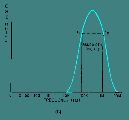 |
A good rule of thumb is that, for faithful (meaning that you can't see the difference using an oscilloscope) reproduction of both amplitude and phase characteristics of a signal, an amplifier should have a -3 db frequency response specification that extends from one tenth of the lowest frequency of your signal to ten times the highest frequency.
| Amplifier manufacturers don't always spell out the methods they use to determine bandwidth; some amplifiers, for instance, may be rated at the "3 dB down" points. These are the upper and lower frequencies at which output falls below the rated power by more than 3 dB. Because this figure is not clearly definitive, the prospective buyer should know how the designer has arrived at his specification. For this reason, an amplifier may be viewed as a low pass filter with gain and the filter terminology of passband ripple, group delay, phase delay, transition band, stopband, stopband ripple, etc. will give a more precise model of the amplifier. | 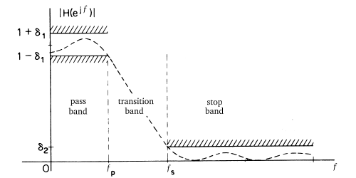 |
|
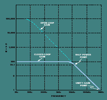
Open Loop Bandwidth is the bandwidth of the amplifier with no AC feedback applied. In a gain stage there is a limit to the achievable bandwidth at some set gain. This means the higher the gain, the lower the bandwidth; conversely, the lower the gain, the wider the bandwidth. This is the now famous, Gain Bandwidth Product ( GAIN X BANDWIDTH = UNITY GAIN POINT ).
|  |
Using the subcircuit, we can determine the gain bandwidth of a 0.1 ac voltage input. The analysis file tut_spice3_jfet_bias_ac.cir applies a test circuit for analysis.
unix> spice3 tut_spice3_jfet_bias_ac.cir

Spice 1 -> run

Spice 2 -> plot -vdb(vout)

Spice 3 -> plot vp(vout)
Line 1 runs the ac analysis declared in the spice file. The run command first computes the dc operating point of the circuit (.OP) and determines linearized, small-signal models for all of the nonlinear devices in the circuit. The resultant linear circuit is then analyzed over a user-specified range of frequencies.
The spice statement .AC DEC 100 1 1T says to do 100 point analysis for every log decade in the circuit starting from 1 Hertz to 1 TeraHertz. This will also cause the default plot to be a log (not linear) plot. In order to get a Bode plot of the frequency response use the functions vdb(...) and vp(...) for magnitude (decibels) and phase plot. In Line 2, since the amplifier inverts the negative decibels of Vout is plotted (i.e. -vdb(...)). Line 3 plots the phase plot of the amplifier. The gain bandwidth of the amplifier is when it crosses the zero axis.
Now let us increase the input voltage amplitude to 4 volts and rerun the ac analysis.
Spice 4 -> show all


 JFET: Junction Field effect transistor
 device     j:amp1:1
 model     amp1:j2n3
       vgs     -1.01
       vgd     -12.2
        ig -1.33e-11
        id   0.00532
        is  -0.00532
       igd -1.22e-11
        gm   0.00533
       gds  1.17e-05
       ggs  1.03e-12
       ggd     1e-12

 Resistor: Simple linear resistor
 device     r:amp1:g  r:amp1:s  r:amp1:d     rload
 model             R         R         R         R
resistance     1e+06       188  1.46e+03     1e+06
         i     1e-07  0.000529 -6.84e-05  9.99e-08
         p     1e-08  5.26e-05  6.83e-06  9.99e-09

 Vsource: Independent voltage source
 device           v1       vdd
        dc         0        20
     acmag       0.1         0
         i -0.000598  6.84e-05
         p  5.98e-05        -0

Spice 5 -> alter V1 acmag = 4

Spice 6 -> run

Spice 7 -> plot -vdb(vout)

Spice 8 -> plot vp(vout)
Line 4 shows all the devices and their parameters which can be used by the alter command. Line 5 alters the "V1 Vin 0 DC 0 AC 0.1" statement to "V1 Vin 0 DC 0 AC 4" without using and editor and reloading the circuit file. Line 6, reruns the current ac analysis. Line 7 and 8 displays the new plot.
The bandwidth is the same. Does this make sense. A 4 volt input should overload the output. Let's see if that is true. The follow shows a single sine wave applied to the input at 0.1 and a 6 volts input signal using the two files tut_spice3_jfet_bias_sine1.cir and tut_spice3_jfet_bias_sine6.cir.
unix> spice3 tut_spice3_jfet_bias_sine1.cir

Spice 1 -> run

Spice 2 -> plot vout

Spice 3 -> plot i(vdd)

Spice 4 -> fourier 1e6 Vout


Fourier analysis for Vout:
  No. Harmonics: 10, THD: 0.286003 %, Gridsize: 200, Interpolation Degree: 1

Harmonic Frequency   Magnitude   Phase       Norm. Mag   Norm. Phase
-------- ---------   ---------   -----       ---------   -----------
 0       0           12.2045     0           0           0
 1       1e+06       0.383539    179.655     1           0
 2       2e+06       0.00109508  88.4973     0.00285521  -91.158
 3       3e+06       2.54643e-05 -107.95     6.63929e-05 -287.6
 4       4e+06       2.39938e-05 -91.007     6.2559e-05  -270.66
 5       5e+06       2.38823e-05 -91.271     6.22683e-05 -270.93
 6       6e+06       2.38175e-05 -91.465     6.20994e-05 -271.12
 7       7e+06       2.37761e-05 -91.632     6.19914e-05 -271.29
 8       8e+06       2.37342e-05 -91.858     6.1882e-05  -271.51
 9       9e+06       2.36566e-05 -92.086     6.16798e-05 -271.74

Spice 5 -> source tut_spice3_jfet_bias_sine4.cir

Spice 6 -> run

Spice 7 -> plot vout

Spice 8 -> plot i(vdd)

Spice 9 -> fourier 1e6 Vout


Fourier analysis for Vout:
  No. Harmonics: 10, THD: 37.3013 %, Gridsize: 200, Interpolation Degree: 1

Harmonic Frequency   Magnitude   Phase       Norm. Mag   Norm. Phase
-------- ---------   ---------   -----       ---------   -----------
 0       0           12.4351     0           0           0
 1       1e+06       9.00839     179.515     1           0
 2       2e+06       0.747533    -89.631     0.0829818   -269.15
 3       3e+06       3.0704      179.045     0.340837    -0.46939
 4       4e+06       0.105121    81.2828     0.0116693   -98.232
 5       5e+06       1.08458     178.589     0.120397    -0.92552
 6       6e+06       0.163678    84.0992     0.0181695   -95.416
 7       7e+06       0.265723    179.039     0.0294973   -0.47605
 8       8e+06       0.135003    85.1087     0.0149864   -94.406
 9       9e+06       0.0460269   -10.666     0.00510933  -190.18
Observe that the second plot shows a distorted sine wave. Hence, the bandwidth parameter is not capturing this effect. Line 4 preforms a fourier analysis on the transient analysis. The THD for 0.1 input is 0.28% whereas the THD for the 6 volt input is 37.3%! The fourier command's first argument is the same time as the transient stop time and the second argument is the transient signal node to be analyzed. This command can also be placed in the circuit file as a ".FOUR 1e6 Vout" statement. Line 5 reads in another circuit file which now becomes the current design circuit.
| 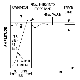 |
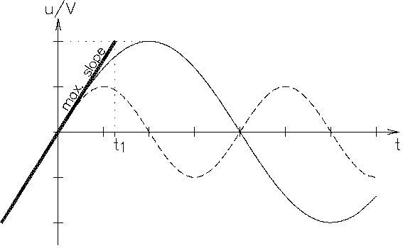
In essence, slew rate is a measure of an amplifier's ability to follow its input signal. It is measured by applying a large amplitude step function (a signal starting at 0 volts and "instantaneously" jumping to some large level [without overshoot or ringing], creating a step-like look on an oscilloscope) to the amplifier under test and measuring the slope of the output waveform. For a "perfect" step input (i.e., one with a rise time at least 100 times faster than the amplifier under test), the output will not be vertical; it will exhibit a pronounced slope. The slope is caused by the amplifier having a finite amount of current available to charge and discharge its internal compensation capacitor.
When reading frequency response specifications, it is also necessary to know at what signal amplitude the given values apply. Also, The slew rate will differ if the amplifier is a inverting or noninverting amplifier. The reason for this is that often a particular device has a very wide frequency response provided that only very small signals are applied, but slew rate limiting causes a much narrower frequency response when a normal signal is applied.
For example, one device is specified as having a frequency response of DC to 150 MHz and a slew rate of 400 V/µs. In this instance, if a signal consisting of a 150 MHz sine wave with a peak amplitude of one volt is applied to the device, the output will be seriously distorted due to the slew rate limitation.
| For a device to pass a sine wave with no distortion, the slew rate of the device must meet or exceed the highest rate of change of the sine wave. This occurs as the sine wave passes through zero going positive or negative and, although the rate of change has a different polarity in the two instances, the magnitude is the same in both instances: |
|
Using the subcircuit, we a step pulse (pwl: piecewise linear) to the input of the amplifier and observe when the output stops rising. The analysis file tut_spice3_jfet_bias_sr.cir applies a test circuit for analysis.
unix> spice3 tut_spice3_jfet_bias_sr.cir

Spice 1 -> run

Spice 2 -> plot vout
References: