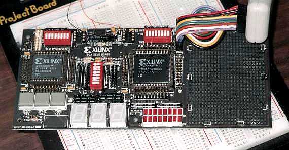
Figure 1: Picture and Schematic layout of the FPGA Demo Board (Ref. Xilinx).
Figure 1: Picture and Schematic layout of the FPGA Demo Board (Ref. Xilinx).
The board is a convenient stand-alone board that contains, in addition to the FPGA chip, a series of switches, LEDs and 7 segment displays that can be used to toggle inputs and display outputs. Figure 1 shows a schematic layout of the board. The board contains a socket for both the XC3000 and the XC4000 84-pin FPGAs. The board will most likely be populated with a XC3020A PC68 and an 84-pin XC4003E or XC4010E PC84 device.
Notice that the FPGA chips are volatile and will need to be reprogrammed everytime you switch off the power supply (unless you program the configuration in a PROM; the demonstration board can be used for this as well). In case you need a non-volatile chip, you can use the 9500 CPLD devices. However, these cannot be programmed with the demonstration board. In that case, you can do in-circuit programming using the XChecker cable or the XC95 board. The rest of this write-up concerns the demonstration board used for programming FPGAs.
After configuration, any input/output pin that is not used, will be configured as an input with a 50-100 kOhm pull-up resistor (connected to the Vdd). Input pins will also be connected to a 50-100kOhm pull-up resistor. This is done on the FPGA device in the IOB block (see FPGA data book).
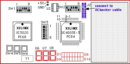
The 8 DIP switches, labeled SW1 and SW2, just above the XC3020 and XC4003
sockets, respectively, are configuration switches(see table below). They
should be set as indicated in the table. For more information about the
meaning of these switches, consult the Xilinx on-line documenation (XACT
docs, Hardware and Peripherals, Chpt. 1).
|
no. |
SW1 (XC3000)
(normal position) |
|
(SW2) |
|
|
INP - | PWR (Power) |
|
|
|
MPE (OFF) | MPE (multiple program conf.; used with PROM) |
|
|
|
SPE (OFF) | SPE (single config.; used with PROM) |
|
|
|
M0 (ON) | M0 (multiple program enable) |
|
|
|
M1 (ON) | M1 (multiple program enable) |
|
|
|
M2 (ON) | M2 (multiple program enable) |
|
|
|
MCLK (OFF) | RST (reset) |
|
|
|
DOUT (OFF) | INIT |
|
NOTE: the switches are ON when the top half is pressed down (towards the number labeled on the swithces).
The 8 DIP swithes positioned vertically between the two sockets (see Figure 1) are general-purpose inputs for both the XC3020A and the XC4003E FPGAs. These are handy to apply input signals to the devices during testing. When the switch is ON (pressed in towards the switch number on the right-half side of the switch) a logic "1" is applied, and a logic "0" when the switch is OFF. Logic "0" is applied through a 4.7Kohm resistor as shown in figure 2 below. The pin connections for the SW3 are shown in the following table. Because the FPGA pin is isolated from the switch by a 1Kohm resistor, the pins can also used as outputs or they can be driven from an external source by connecting the signal source to the FPGA probe point header.
The pin connections for the SW3 are shown in the following table.
|
|
|
|
|
|
|
|
|
|
|
|
|
|
|
|
|
|
|
|
|
|
|
|
|
|
|
|
|
|
|
|
|
|
|
|
General purpose switches SW3 connection:
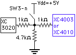
Figure 2: General Purpose swithces SW3-n
The leftmost display is connected to the XC3010A FPGA while the two
right most ones are connected to the XC4003E chip. Each LED segment is
swithced on by driving the corresponding pin
"LOW". The pin
I/O connections of the 7-segment display are shown in the following table
and Figure 3.
|
|
|
|
|
|
|
|
|
|
|
|
|
|
|
|
|
|
|
|
|
|
|
|
|
|
|
|
|
|
|
|
|
|
|
|
|
|
|
|
|
|
|
|
|
|
|
|
|
|
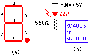
Figure 3: 7-Segment display: (a) LED segments and (b) LED connection
Each LED is turned on by driving the corrsponding FPGA pin "LOW". Thus
the LEDs are active low. The LED connections are shown in Fig. 3b.
The decimal point of the rightmost display (U8) is connected to pin 41 of the XC4003E and acts as a programming error indicator. During proamming the decimal point of U8 should be off. If it comes back on, there has been a programming error. The decimal points of U6 and U7 are tied low during programming and are on when the FPGAs are waiting to be programmed.
The LEDs below the XC4003 socket (see
Fig. 1) are connected to the I/O pins of the FPGA. The top 8 LEDs (D1-D8)
are connected to the XC3020A, the lower 8 LEDs are connected to the I/O
pins of the SC4003 or XC4010. As with the 7-segment display, the LEDs
will be one when a logic "LOW" or "0" is connected to the pin (i.e.
asserted low as shown in Fig 3b.). The table below
gives the pin numbers.
|
|
|
|
|
|
|
|
|
|
|
|
|
|
|
|
|
|
|
|
|
|
|
|
|
|
|
|
|
|
|
|
|
|
|
|
|
|
|
|
|
|
|
|
|
There are additional 16 I/O lines available on the two rows of pins
(headers for probe points) above the XC4003 or 4010 device. The pin numbers
are given in the following table, starting from left to right. Pin numbers
increase from the inside row to the outside, counter-clockwise (see Fig.
1 or Fig 4). After configuration, any input/output pin that is not used,
will be configured as an input with a 50-100 kOhm pull-up resistor (connected
to the Vdd). Input pins will also be connected to a 50-100kOhm pull-up
resistor. This is done on the FPGA device in the IOB block (see FPGA data
book).
|
|
|
|
|
|
|
|
|
|
|
|
|
|
|
|
|
|
|
|
|
|
|
|
|
|
|
|
|
|
|
|
|
|
|
|
|
|
|
|
|
|
|
|
|
|
|
|
|
|
|
|
|
|
|
|
|
|
|
|
|
|
|
|
|
|
|
|
Pin numbers on the FPGA demoboard:
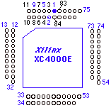
Figure 5: FPGA pin numbers of the XC4000 device on the demoboard (numbers increase from the inside row to the outside one, counter-clockwise).
SW4 is a reset button which applies an active "LOW" Reset Signal to the FPGA or the PROM. Reset is normally pulled "High" through a 27Kohm resistor
SW5 is a spare pushbotton that applies an active "LOW" to pin 18 of the XC4003 ir XC4010 and to pin 16 of the XC3020. Normally the spare signal is pulled "HIGH".
SW6 is the program pushbotton which applies an active "LOW" signal to the DONE/PROGRAM input on the XC4003 (or XC4010) at pin 55 or at pin 45 of the XC3020. The PROG signal is usually pulled high through a 13.5 KOhm resistor.
Below the PROG pushbutton SW6 there is a spare place for an oscillator. The oscillator output will be connected to pin 13 (PGCK1 pin) of the XC4003 and to pin 43 of the XC3020 FPGA.
The other pins are used for programming and powering the FPGAs. The VCC (=5V) and GND pins are listed below for the XC4003 PC84 FPGA:
GND: pins 1, 12, 21, 31, 43, 52, 64, 76
GND: pin 35
The XChecker cable (connected to me parallel printer port) should be connected to connector J2 (the vertically-placed connector pins at the top right side of board) to program the XC4003 or to connector J1 (left top side) for programming the XC3020. These connectors are missing a pin in the third position of the left vertial row and a pin in the fourth position of the right row. The XChecker has two flying lead connectors (tiny wires with labels on the side) and have the same pin numbers missing. This allows you to connect the cable correctly to the demoboard connector. Notice that the position of the symbols written on top of the XChecker head are mirrored from what the actual pins mean. The correct names are indicated on the flying leads connected to the cable.